MIT research team discovers how to keep Moore’s Law alive using 2D materials grown on silicon wafers

Gordon Moore, the co-founder and former CEO of Intel, made an observation in 1965 that the number of transistors on a chip doubles every year. In 1975, he revised his “law” calling for the number of transistors on a chip to double every other year. Typically, the higher a chip’s transistor count the more powerful and energy-efficient it is.

With the leading process node currently at 3nm, both TSMC and Samsung Foundry have plans to drop down to 2nm by 2025. Samsung has said that its road map includes a 1.4nm node in 2027. But eventually, silicon loses its electrical characteristics at a certain size and Moore’s Law could be repealed (yes, we know that it isn’t a real law).

The use of 2D materials to build small transistors could keep Moore’s Law alive
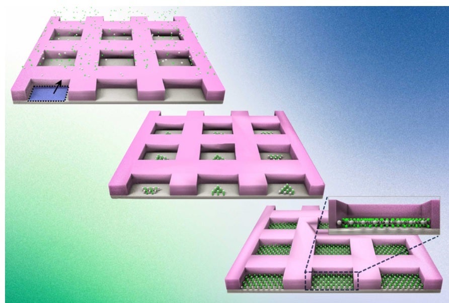
One possible way to keep Moore’s Law alive has been floated by a team of researchers at MIT. The team discovered that it could build smaller transistors by using 2D materials. Using a method called “nonepitaxial, single-crystalline growth,” 2D materials are grown on silicon wafers. These 2D materials are ultra-thin two-dimensional sheets of perfect crystals as thin as one atom. The MIT team says that the 2D materials it created were free of any defects allowing it to create a simple, functional transistor.

The 2D materials are known as transition-metal dichalcogenides, or TMDs. At nanometer scale, they conduct electrons more efficiently than silicon.

This could be the breakthrough that the tech industry needs to continue building more powerful chips. As an example of how Moore’s Law works, consider that in 2019, Apple’s 5nm A13 Bionic chipset, used to power the iPhone 11 line, carried 8.5 billion transistors. The 4nm Apple A16 Bionic SoC, found in the iPhone 14 Pro models, each were equipped with close to 16 billion transistors.
It is widely expected that this year, Apple’s premium iPhone 15 models will use the A17 Bionic which will be produced using the 3nm process node; the chip could carry anywhere from 18 billion to 20 billion transistors or more.

Speaking about the use of 2D materials to keep Moore’s Law alive, Jeehwan Kim, associate professor of mechanical engineering at MIT, said, “We expect our technology could enable the development of 2D semiconductor-based, high-performance, next-generation electronic devices. We’ve unlocked a way to catch up to Moore’s Law using 2D materials.”

The MIT researchers were able to overcome the difficult task of growing 2D materials on silicon

The team was able to overcome the challenge of growing 2D materials on silicon. To build semiconductors, silicon wafers must be used, the associate professor noted. “Until now, there has been no way of making 2D materials in single-crystalline form on silicon wafers, thus the whole community has almost given up on pursuing 2D materials for next-generation processors,” Kim says. “Now we have completely solved this problem, with a way to make devices smaller than a few nanometers. This will change the paradigm of Moore’s Law.”

Other areas of research that Intel will focus on include looking into new 3D packaging for seamless integration of chiplets, and studying new possibilities in energy efficiency and memory. As for the use of 2D materials, Intel says that these super-thin materials can help it fit more transistors inside a single chip.

Transistors made from 2D materials could be the innovation that keeps the tech industry growing. It might allow manufacturers to develop faster and more powerful smartphones with the kind of battery life that we can only dream about right now.

For all the latest Technology News Click Here 

 For the latest news and updates, follow us on Google News

Read original article here

Denial of responsibility! TheDailyCheck is an automatic aggregator around the global media. All the content are available free on Internet. We have just arranged it in one platform for educational purpose only. In each content, the hyperlink to the primary source is specified. All trademarks belong to their rightful owners, all materials to their authors. If you are the owner of the content and do not want us to publish your materials on our website, please contact us by email – [email protected] The content will be deleted within 24 hours.