Accelerating nanoscale X-ray imaging of integrated circuits with machine learning

Researchers from MIT and Argonne National Laboratory have developed a machine learning technique that could greatly accelerate the process of nanoscale X-ray imaging of integrated circuits, potentially revolutionizing the way we manufacture and test electronics.
Integrated circuits, or microchips, are the building blocks of modern electronics, and their continued miniaturization has led to increasingly complex and powerful devices. However, as the components of these microchips shrink, it becomes more difficult to inspect and test them using traditional imaging techniques.
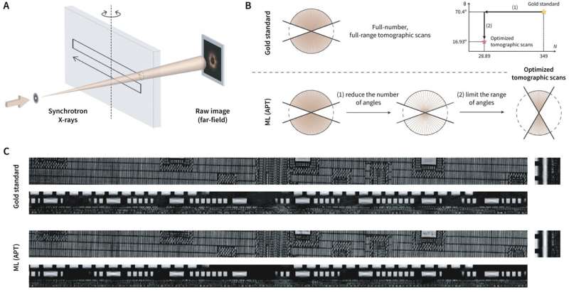
One promising method for imaging nanoscale components is synchrotron X-ray ptychographic tomography, which uses high-energy X-rays to penetrate the material and create detailed images of the internal structure. However, X-ray imaging is a slow process that requires precise positioning of the sample and the detector, and can take hours or even days to get a single reconstruction.
To speed up this process, the MIT and Argonne researchers turned to machine learning. They trained a neural network to predict accurate reconstructions of the objects in a fraction of the time it would normally take. Their network is called APT or Attentional Ptycho-Tomography, which utilizes regularizing priors in the form of typical patterns found in integrated circuit interiors, and the physics of X-ray propagation through the object.
“The neural network is able to learn from a small amount of data and generalize, which allows us to image and reconstruct the integrated circuits quickly,” said Iksung Kang, the lead author of the paper. The researchers noted that their approach significantly reduces the total data acquisition and computation time needed for imaging. They tested their technique on a real integrated circuits and were able to capture detailed images in just a few minutes, compared to the hours it would normally take.
“This new method could be an effective solution for quality assurance,” they said. “By accelerating the imaging process, we can also enable fabs to connect to synchrotron X-ray sources.”
The researchers noted that their approach could have significant implications for a variety of fields, including materials science and biological imaging. “Our research addresses a critical challenge in noninvasive X-ray imaging of nanoscale objects, such as integrated circuits,” said the lead author. “We believe that our physics-assisted and attention-utilizing machine learning framework could be applicable to other branches of nanoscale imaging.”
The work is published in the journal Light: Science & Applications.
More information:
Iksung Kang et al, Attentional Ptycho-Tomography (APT) for three-dimensional nanoscale X-ray imaging with minimal data acquisition and computation time, Light: Science & Applications (2023). DOI: 10.1038/s41377-023-01181-8
Citation:
Accelerating nanoscale X-ray imaging of integrated circuits with machine learning (2023, June 1)
retrieved 2 June 2023
from https://phys.org/news/2023-06-nanoscale-x-ray-imaging-circuits-machine.html
This document is subject to copyright. Apart from any fair dealing for the purpose of private study or research, no
part may be reproduced without the written permission. The content is provided for information purposes only.
For all the latest Science News Click Here
For the latest news and updates, follow us on Google News.

