Clean doping strategy produces more responsive phototransistors

The library of two-dimensional (2D) layered materials keeps growing, from basic 2D materials to metal chalcogenides. Unlike their bulk counterparts, 2D layered materials possess novel features that offer great potential in next-generation electronics and optoelectronics devices.
Doping engineering is an important and effective way to control the peculiar properties of 2D materials for the application in logical circuits, sensors, and optoelectronic devices. However, additional chemicals have to be used during the doping process, which may contaminate the materials. The techniques are only possible at specific steps during material synthesis or device fabrication.
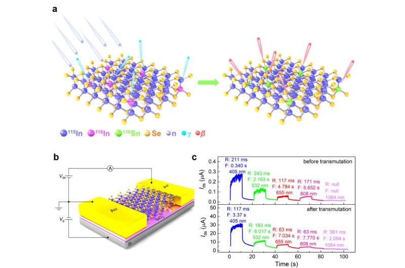
In a new paper published in eLight, a team of scientists led by Professor Han Zhang of Shenzhen University and Professor Paras N Prasad of the University of Buffalo studied the implementation of neutron-transmutation doping to manipulate electron transfer. Their paper, titled has demonstrated the change for the first time.
Neutron transmutation doping (NTD) is a controllable in-situ substitutional doping method that utilizes the nuclear reactions of thermal neutrons with the nuclei of the atoms in semiconductors. It provides a new way to dope 2D materials intentionally without extra reagents. NTD can be introduced into any step during the fabrication of 2D-materials-based devices, or even used post-fabrication.
NTD was successfully developed in 1975 for bulk semiconductors like Si, gallium phosphide (GaP), and indium phosphide (InP). In 1991, the tin(Sn)-related shallow donors could be uniformly introduced into the bulk indium selenide (InSe) crystal by NTD. The further performance improvement of the 2D layered InSe based photodetectors is limited by the low carrier density of the doped InSe. It would be fascinating if 2D layered InSe based photodetector performances could be manipulated and optimized via the “clean” method of NTD.
The research team realized the doping of 2D layered InSe via NTD for the first time. They successfully narrowed the bandgap and increased the electron mobility of SN-doped layered InSe, reflecting a significant improvement. They raised the field-effect electron mobility from 1.92 cm2 V-1 s-1 to 195 cm2 V-1 s-1. At the same time, the photodetector’s responsivity improved by about fifty times to 397 A/W.
The research team believes that NTD holds enormous promise for the future of materials research. It should enable significant new opportunities in materials-based technologies. Under the NTD method, dopants can be strictly controlled and introduced at any time, which will improve efficiency. By doping at the atomic level, researchers and industries can ensure that dopants are placed in exactly the right place and know the precise impact of the dopant in that location. Finally, NTD could be used to protect people, particularly when sensing gases or other biological issues.
High performance polarization sensitive photodetectors on 2D semiconductor
Zhinan Guo et al, In-situ neutron-transmutation for substitutional doping in 2D layered indium selenide based phototransistor, eLight (2022). DOI: 10.1186/s43593-022-00017-z
Citation:
Clean doping strategy produces more responsive phototransistors (2022, June 7)
retrieved 7 June 2022
from https://phys.org/news/2022-06-doping-strategy-responsive-phototransistors.html
This document is subject to copyright. Apart from any fair dealing for the purpose of private study or research, no
part may be reproduced without the written permission. The content is provided for information purposes only.
For all the latest Science News Click Here
For the latest news and updates, follow us on Google News.

